

-
December 9, 2026
Event date:
-
December 11, 2026
Event end:
Overview
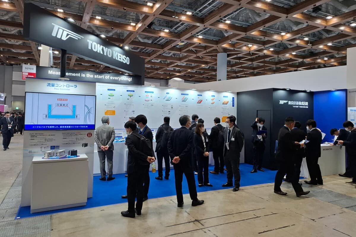
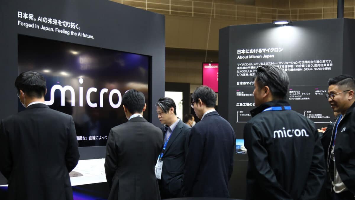
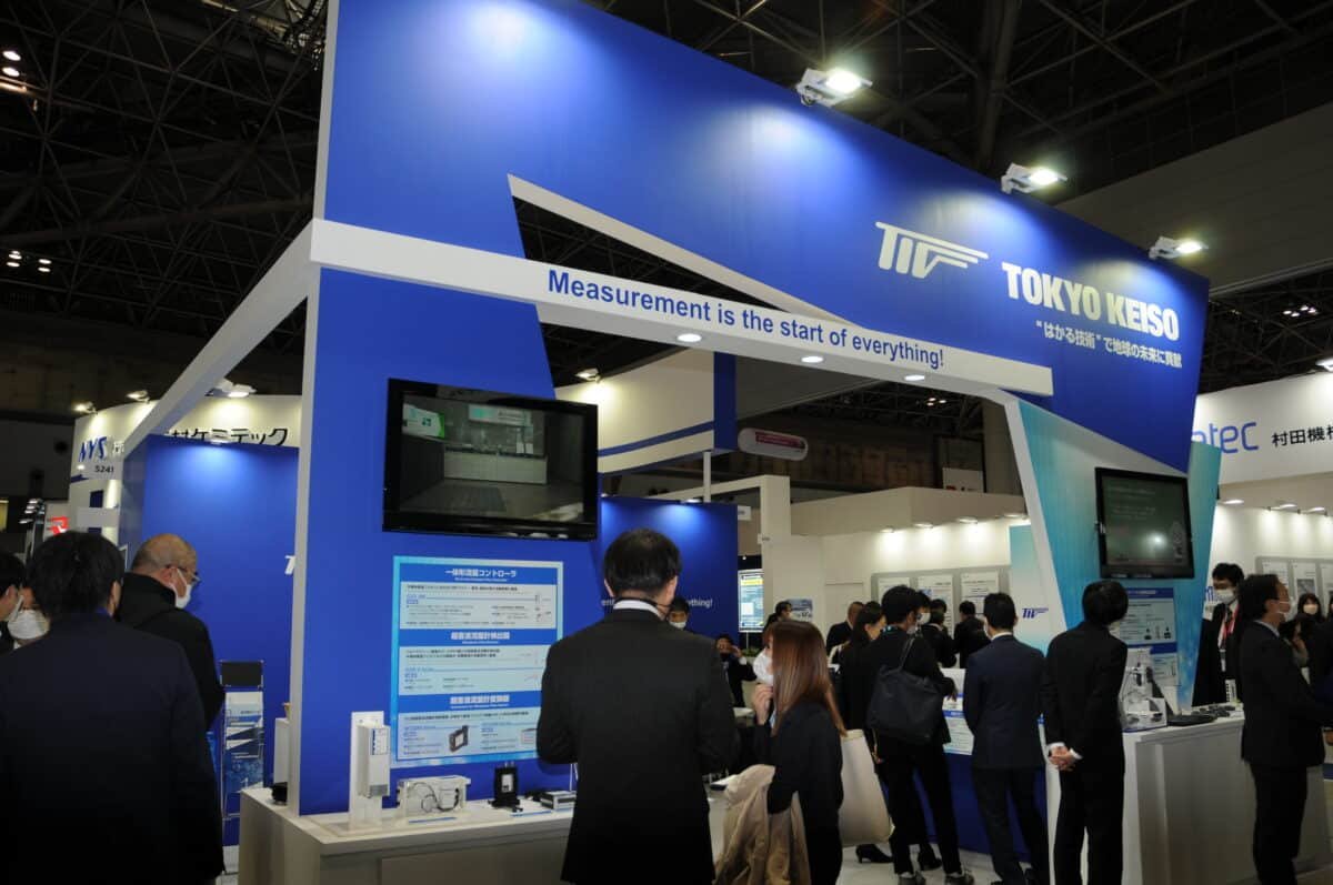
SEMICON Japan 2026 stands as one of the most prominent international business-to-business exhibitions and technical conferences dedicated entirely to the semiconductor manufacturing supply chain, microelectronics, and advanced packaging systems. Held annually at Tokyo Big Sight, this landmark three-day trade show serves as a critical commercial crossroads connecting chip designers with equipment developers. The massive exhibition floor brings together over one thousand leading global companies showcasing groundbreaking solutions in photolithography, chemical mechanical planarization, plasma etching, and silicon wafer processing. It functions as an essential corporate platform designed to accelerate industrial digital transformation, stabilize microchip supply chains, and foster cross-border technology transfers.
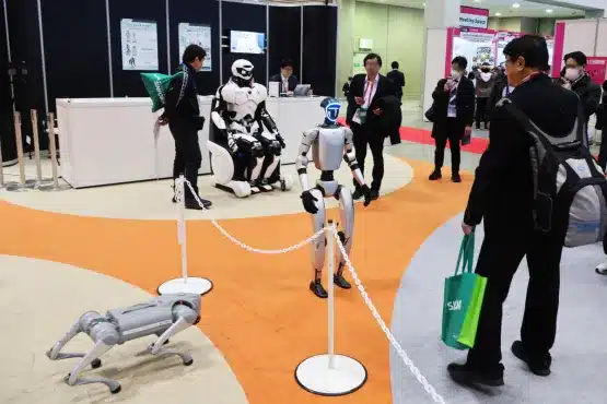
The comprehensive exhibition layout features highly specialized technological zones tailored to facilitate strategic procurement and advanced business matching. Visitors can explore massive pavilions showcasing atomic layer deposition machinery, precision metrology equipment, high-purity processing chemicals, and advanced glass carrier substrates for next-generation chiplet packaging. Furthermore, the exposition features extensive presentations focusing on smart applications powered by semiconductor technology, such as autonomous vehicles, Internet of Things networks, and generative artificial intelligence hardware. This immense concentration of technology enables commercial enterprises from electronics manufacturing, aerospace components, and telecommunications sectors to find tailored microelectronic manufacturing solutions.
Beyond the physical hardware displays, the event functions as an elite educational and executive networking hub, hosting a rigorous program of global leadership theater sessions and technical summits. Attendees gather to hear from national industrial policy officials, global foundry executives, and elite materials science researchers outlining future manufacturing roadmaps and sustainability initiatives. The energetic trade environment promotes immediate face-to-face commercial negotiations, joint venture formations, and major procurement contract signings between Tier-One suppliers and device makers. For corporate executives, microchip engineers, and tech pioneers alike, this specialized exhibition remains an indispensable destination for securing an early competitive advantage in the global electronics market.
Enjoy Your Event Stress-Free with Japan Travelo
Do you know? Planning events, festivals, concerts, and cultural experiences in Japan can be overwhelming. Japan Travelo brings everything together in one place, helping you manage your itinerary, transport, and accommodation with ease—so you can enjoy Japan without the stress of planning.
Event Highlights
- Advanced Packaging and Chiplet Summit: A highly anticipated dedicated pavilion showcasing innovative microvias, glass core substrates, and multi-die bonding technologies driving next-generation performance.
- SuperTHEATER Global Leadership Keynotes: A prestigious presentation arena hosting top executives from major international foundries and technology ministers debating future geopolitical microchip policies.
- Metrology and Inspection Summit Center: A specialized technical hub highlighting automated defect detection systems, high-resolution electron microscopes, and advanced optical wafer inspection tools.
- Workforce Development and Talent Pavilions: A dynamic interactive zone connecting university engineering students with leading global semiconductor corporations to address industry talent shortages.
Why Attend
This monumental microelectronics trade exhibition provides an unparalleled business environment for corporate leaders to secure direct component supply chains and integrate advanced manufacturing solutions into their operations. It is ideal for foundry chief engineers, electronics procurement executives, venture capitalists, national trade policy directors, and materials science researchers looking to expand their industrial networks. Attending empowers you to evaluate thousands of commercial systems simultaneously and engage directly with primary equipment fabricators.
The commercial advantages of participating extend to establishing vital direct business alliances within the international microelectronics supply chain and discovering niche chemical components before they reach mainstream distribution channels. You can engage directly with technical scientists to learn about the latest trends in extreme ultraviolet lithography calibration and low-damage plasma etching processes. Interacting with elite global thinkers enables attendees to optimize their corporate development strategies, mitigate cross-border supply chain risks, and unlock brand-new market pathways.
Date & Duration
- Event Date: December 9 to December 11, 2026
- Event Duration: Three days of intensive commercial trading, technical panels, and global executive networking
Visiting this event? Don’t miss out on these amazing activities and local experiences while you’re here.
Ticket Information
- How Tickets Are Sold: Registration is processed exclusively online through the official trade exposition website where business visitors must secure their admission credentials before arrival.
- Admission Type: Free Admission for verified corporate professionals, microchip engineers, hardware researchers, government personnel, and trade visitors who complete the mandatory pre-registration.
- Ticket Pricing: Approved professional digital visitor badges cost 0 dollars, while general consumers and members of the public without verifiable microelectronics business interests are barred from entering.
- Special Seating Options: Standard seating inside the tech theaters, forum rooms, and presentation stages is open to all badge holders on a first-come basis with no advanced reservations required.
- VIP Options: Premium VIP registration configurations are allocated specifically to key corporate sponsors, keynote speakers, and senior management from major device manufacturing firms.
Venue / Location
- City and Country: Tokyo, Japan
- Venue Name: Tokyo Big Sight
- Google Maps Address: 3 Chome-11-1 Ariake, Koto City, Tokyo 135-0063, Japan
Contact Information
- Email: jmarketing@semi.org
- Phone Number: +81-3-3222-5755
- Official Website: https://www.semiconjapan.org/en
- Social Media Links:
- https://twitter.com/semicon_jpn
- https://www.facebook.com/SEMICONJAPAN/
- https://www.linkedin.com/company/semi-japan
- https://www.youtube.com/channel/UCoK1IVdR_3e_4g2vF8KSj7w
Getting There
- Nearest Airport: Tokyo Haneda International Airport is situated roughly 15 kilometers away from the main convention complex and can be reached swiftly via road transport lines.
- Nearest Train/Metro Station: Kokusai-Tenjijo Station on the Rinkai Line and Tokyo Big Sight Station on the Yurikamome Monorail line are located within immediate short walking distance.
- Bus Routes or Public Transport Options: Toei city transit buses offer direct transit services connecting central railway hubs like Tokyo Station and Toyosu Station straight to the central exhibition plaza.
- Parking Availability: Multiple massive public vehicular parking structures surround the Tokyo Big Sight convention center grounds, accommodating private corporate vehicles and regional shuttle buses.
- Directions by Car: Drivers originating from central Tokyo districts should take the Metropolitan Expressway Route 11 Daiba Line and take the designated Ariake exit to approach the venue.
What is this event?
SEMICON Japan 2026 is the nation’s largest professional business-to-business trade exhibition and technical conference focused exclusively on the semiconductor manufacturing supply chain, materials science, and electronic design components. It serves as a unified corporate marketplace where international hardware suppliers present their newest fabrication systems to semiconductor device manufacturers.
The event encompasses massive multi-hall exhibition spaces filled with technical supplier booths, active equipment demonstration zones, and dedicated leadership theater stages. It operates purely as a professional networking, business matching, and technical procurement platform aimed at expanding cross-industry collaborations worldwide.
Why is it popular?
The event is highly popular because it addresses the rapid global expansion of chip fabrication by serving as a singular meeting point for international toolmakers and regional foundry operators. It has gained an outstanding reputation over four decades for showcasing critical equipment innovations that drive the evolution of global consumer electronics.
Its popularity is further elevated by the inclusion of specialized concurrent summits like the Advanced Packaging Summit and the free-to-attend technical keynotes. Corporate developers flock to the venue to discover how advanced packaging substrates and chemical engineering solutions can maximize the processing power of artificial intelligence hardware.
Tips before you go
- Complete your digital visitor profile on the official website beforehand to download your entry badge and avoid long queues at the venue verification counters.
- Wear highly comfortable professional footwear as navigating all the massive multi-district exhibition halls and technical conference areas requires extensive walking.
- Prepare a generous supply of corporate business cards to exchange with international equipment manufacturers and domestic chemicals suppliers during networking sessions.
- Review the schedule of live theater presentations before arriving so you can plan your day around the specific executive panels that match your corporate goals.
- Bring a sturdy tote bag or rolling sample case to comfortably transport the numerous technical catalogs, data booklets, and material specifications you will gather.
Attendee Experiences
- Sourcing the new glass core packaging substrates directly from the material developers allowed our technology firm to optimize its AI chiplet architecture plans.
- Listening to global foundry executives analyze international supply chain dependencies on the main stage provided incredible, actionable market intelligence.
- The pre-registration process was completely seamless and the proximity of the monorail station made commuting from our hotel highly efficient.
Video
Location
FAQ
What are the specific daily opening and closing hours for the exhibition halls?
The exhibition center doors open to registered trade visitors starting at ten o'clock in the morning on all three event days. The technical booths, presentation stages, and business networking zones remain fully active until five o'clock in the afternoon when the halls close for the evening.
Are there any advanced registration fees required to attend the global leadership theater keynotes?
All of the expert conference presentations, panel discussions, and technical semiconductor summit sessions are entirely free to attend for any registered visitor. There are no individual ticketing fees for the educational stages, though you must possess a valid general event entry badge to access the halls.
Is there multi-lingual support available for international corporate buyers during the technical seminars?
The event management office provides comprehensive multi-lingual signage, international information desks, and professional translation assistance throughout the main exhibition complex. Major international leadership conferences and global roundtable presentations also utilize simultaneous interpretation systems supporting both Japanese and English languages.
Can companies from non-semiconductor sectors benefit from visiting this technology expo?
A major focus of the exhibition is connecting microelectronic solution providers with mainstream commercial entities from automotive, medical technology, and communications industries. Non-semiconductor businesses can discover unique ways to implement advanced sensors, processing units, and smart technology systems to improve their own commercial operations.
Is it possible to register multiple corporate colleagues under a single application profile?
The online registration system requires each individual attendee to complete a separate visitor application profile to verify their professional industry credentials. Each corporate colleague will receive a unique personalized digital entry pass containing a specific barcode that must be printed out prior to arriving at the venue.

Leave a Reply